
Optical circuit switching acts as a high-speed operator, routing data across massive clusters without the power consumption of traditional packet switching. This development arrives as the landscape of modern high-performance computing undergoes a radical transformation, primarily driven by the insatiable demand for larger and more powerful artificial intelligence clusters. As industry leaders push the boundaries of scale-up architectures, the physical infrastructure supporting these systems is reaching a critical breaking point. This shift is not merely a preference for better performance but a physical necessity as the distance and speed requirements of data transmission begin to exceed the inherent capabilities of traditional copper wiring. At the heart of this transition is the need for fully optical scale-up networks to replace traditional interconnects. Current state-of-the-art systems rely on miles of copper flyover cables to manage internal communication between hundreds of GPUs. However, as data rates climb toward 400 Gbps and beyond, electrical signals suffer from extreme attenuation.
Overcoming the Physical Constraints of Copper
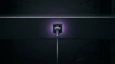
The primary challenge facing next-generation architectures containing over a thousand GPUs is the sheer physical bulk of cabling. In a standard high-scale rack, the volume of copper required becomes unmanageable and creates significant airflow and maintenance issues. While optics solve the signal integrity problem, they introduce a new challenge regarding fiber density. A single high-scale rack could potentially require thousands of fiber pairs, leading to a complex sprawl that is difficult to terminate and manage within the tight confines of a data center. To address this, the industry is focusing on ultra-dense fiber connectivity as a critical first step. New connector technologies are being developed to pack sixty-four or even one thousand fibers into a single, compact interface. This level of density is a prerequisite for any company attempting to build large-scale networks using optics. Without these innovations, the backplanes of modern racks would be physically overwhelmed, making the transition to an optical fabric impossible.
Signal degradation over copper is no longer a manageable engineering hurdle but a hard physical wall that restricts the growth of AI training clusters. At modern data rates, an electrical signal can only travel a little over a meter before the data becomes unreadable, effectively tethering high-speed chips to an incredibly small radius. This limitation forces designers to stack components with extreme density, leading to thermal management nightmares that threaten the stability of the entire system. By transitioning to fiber optics, data centers can extend their reach without sacrificing bandwidth or latency, allowing for more flexible physical layouts. Furthermore, the reduction in signal interference provided by optical fiber means that error correction overhead is lowered, which directly contributes to higher throughput. The shift toward photonics represents a fundamental change in how hardware engineers perceive distance in a data center, turning meters of physical separation into negligible barriers for high-speed communication.
The Strategic Roadmap for Optical Integration
The evolution of optical engines follows a pragmatic, phased approach to how light-based communication is integrated into the silicon itself. The first phase involves Near-Packaged Optics, which places the optical engine close to the GPU or switch while maintaining it as a separate, replaceable component. This strategy allows for easier repairs and refurbishments if a component fails, ensuring that an expensive GPU does not become a total loss due to a minor optical failure. Engineers are currently refining these modules to ensure they can withstand the rigorous thermal cycles of intensive AI workloads. By decoupling the optical engine from the main ASIC, manufacturers maintain a degree of flexibility that is crucial during this transitional period. This approach provides a safety net for hyperscalers who are wary of the yield issues associated with permanent integration. As these technologies mature between 2026 and 2028, they will provide the empirical data needed to justify the next leap in hardware complexity.
The ultimate goal for the end of the decade is Co-Packaged Optics, where the optical engine is integrated directly into the silicon package. By moving the optics to within millimeters of the chip, the need for power-hungry serializer-deserializer components is eliminated, which traditionally accounts for a significant portion of a chip’s power budget. This integration represents the final frontier of interconnect technology, as it bypasses the physical limits of electrical signaling entirely, allowing for maximum efficiency in the world’s largest AI superclusters. Moving optics directly onto the substrate requires sophisticated manufacturing techniques like 2.5D or 3D packaging, but the benefits in power savings and signal density are undeniable. This paradigm shift will likely redefine the role of traditional networking companies, as they transition from selling standalone switches to providing integrated silicon solutions. The consolidation of photonics and electronics into a single package marks the beginning of an era where light and electricity work in perfect unison.
Reimagining Network Topology and Switching
Beyond individual engines, the industry is moving toward high-density Optical Circuit Switching to manage massive GPU clusters. Current switching technology is often limited by a low number of ports, but the next generation of appliances aims to support thousands of ports. These switches route connections between different parts of a cluster without the need for traditional, power-intensive packet switching. To manage this complex web of light, advanced software control planes are required to schedule reconfigurations and ensure seamless data flow. This represents a significant departure from the static networking architectures of the past, where paths were fixed and changes required manual intervention. The ability to dynamically reconfigure optical paths allows data centers to optimize their resources for specific tasks, whether it be large-scale model training or rapid inference. This flexibility is essential for maintaining high utilization rates across thousands of expensive accelerators, ensuring that no GPU sits idle while waiting for data to arrive.
This shift enables a move away from multi-tiered, complex network topologies toward flatter structures. Traditional clusters often require data to take multiple hops to reach its destination, which increases latency—a major problem for modern AI architectures like Mixture-of-Experts. By utilizing high-radix optical interconnects, it is possible to achieve one-hop connectivity across an entire cluster. This allows every GPU to communicate directly with every other GPU, significantly reducing latency and increasing the efficiency of data-heavy AI training. A flatter network also simplifies the physical management of the data center, reducing the number of failure points and making it easier to scale horizontally. As these clusters continue to grow, the importance of minimizing hops cannot be overstated, as every microsecond of delay compounds into hours of lost training time. The implementation of optical fabrics effectively turns an entire data center into a single, massive supercomputer where distance no longer dictates the speed of data transmission.
Market Execution and the Path to Deployment
The success of this optical transition depends heavily on market timing and pragmatism. The history of photonics is filled with startups that failed because they were too early for the market or lacked the manufacturing scale to meet global demand. Today’s leaders are intentionally aligning their product releases with the projected demand of hyperscalers. They are not focused on mere proofs of concept but are building components intended for immediate deployment in the world’s largest data centers to meet the inevitable copper wall. This strategic alignment ensures that the transition to optical interconnects happens in lockstep with the release of next-generation AI accelerators. By coordinating with major silicon providers, photonics companies are ensuring that their connectors and switches are compatible with the hardware being deployed today. This collaborative environment reduces the risk of vendor lock-in and fosters a more competitive market where innovation is rewarded. The focus has shifted from research to industrial reliability.
As the industry moved toward the end of the decade, the transition to light-based systems was no longer a theoretical debate but a commercial certainty. Decision-makers recognized that scaling AI infrastructure required a fundamental rethink of the physical layer. By focusing on increasing port counts, decreasing latency, and solving the physical constraints of fiber density, technologists successfully positioned themselves as the architects of a new computational era. The foundational technologies developed during the mid-twenties dictated the structure of data centers for years, ensuring that AI infrastructure could continue to scale beyond previous limits. Moving forward, stakeholders should prioritize the adoption of standardized optical interfaces to facilitate interoperability between diverse hardware platforms. Investing in staff training for fiber maintenance and upgrading cooling systems to accommodate integrated photonics was identified as a critical next step for facility managers. These proactive measures ensured that the industry was prepared.