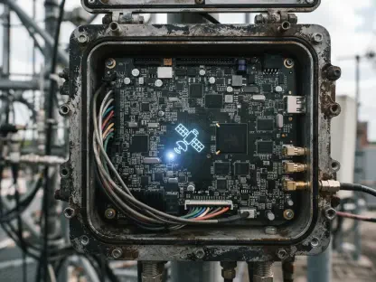

The modern Internet of Things landscape is shifting its focus away from raw connectivity range toward the granular optimization of power consumption and physical footprint at the network edge. Silicon Labs has addressed this fundamental requirement with the launch of the BG2B Bluetooth Low Energy system-on-chip, which represents a significant departure from standard wireless hardware strategies. By prioritizing the internal efficiency of the endpoint rather than simply chasing longer transmission distances, this architecture tackles the persistent challenge of maintaining high-performance connectivity in increasingly compact form factors. This development is particularly relevant as the industry moves toward a massive expansion of connected devices where every milliamp-hour of battery capacity must be strictly conserved. The BG2B serves as a specialized tool for developers who must balance the competing demands of robust wireless performance, advanced security protocols, and minimal physical dimensions.
Strategic Integration: Benefits for Specialized Hardware
Designing advanced hardware often requires a choice between the ease of pre-certified modules and the flexibility of custom system-on-chip solutions. The BG2B is positioned specifically for manufacturers who possess the engineering expertise to develop custom boards from the ground up, allowing them to optimize the layout for specific enclosure constraints. By selecting an SoC rather than a module, these developers can significantly reduce the total bill of materials while gaining much finer control over the device’s energy management profiles. This level of customization is essential for high-volume consumer and industrial products where saving even a few cents per unit or a few millimeters of space translates into a competitive advantage. Furthermore, this approach enables engineers to select specific antennas and passive components that match their unique environmental requirements, leading to a more reliable connection in congested radio frequencies.
The emphasis on high-level integration allows designers to merge the radio, main processor, and various peripheral management tasks into a single, cohesive semiconductor component. This consolidation reduces the overall complexity of the circuit board and frees up critical engineering resources to focus on the software logic and sensor precision that define the product’s value. The transition toward these system-in-a-chip designs reflects a broader industry trend where physical space is treated as a premium commodity and every redundant component is viewed as a liability. By integrating features that once required external components, such as voltage regulation and memory management, the hardware remains exceptionally compact without sacrificing the processing power needed for modern algorithms. This architectural streamlining ensures that the device remains lean while providing the necessary overhead for future firmware updates and long-term functional enhancements.
Economic Sustainability: Security and Implementation Success
Security is treated as a foundational element of the BG2B rather than an optional add-on that could be addressed later in the development cycle. As IoT endpoints are often the most vulnerable parts of a corporate network, integrating security directly into the silicon ensures that even the simplest sensors remain protected against unauthorized access. This built-in approach eliminates the need for external security processors, further reducing both the total cost and the physical complexity of the final hardware design. By establishing a hardware-based root of trust, developers ensure that data integrity is maintained from the moment of capture through to cloud transmission. This high level of protection is achieved without compromising the energy efficiency that defines the chip, proving that robust encryption and low power draw are not mutually exclusive. This integration simplifies the certification process for medical and industrial devices, where data privacy is mandated by strict regulatory frameworks.
The introduction of this high-efficiency silicon highlighted a clear path forward for developers who prioritized sustainable hardware design and long-term operational success. Successful implementation of the technology required engineering teams to re-evaluate their power management firmware to fully exploit the specific low-current modes available in the hardware. Moving through 2026 and toward 2028, the industry successfully integrated these chips into smaller form factors like smart medical patches and logistics labels. Organizations that adopted these SoCs early realized significant reductions in total ownership costs by minimizing the logistical burden of battery maintenance in the field. Technical leaders looked toward hybrid energy solutions, combining this low-power silicon with energy harvesting technologies to create self-sustaining nodes. This strategic pivot provided a foundation for more resilient and economically viable connected ecosystems that operated autonomously for many years.