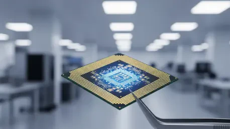

The electromagnetic spectrum has long contained a frustratingly inaccessible territory known as the terahertz gap, a frequency range situated between the microwave and infrared bands that has remained largely untapped due to the physical limitations of existing hardware. Historically, bridging this gap required massive, laboratory-scale setups involving cryogenically cooled lasers and specialized optics that were far too cumbersome for any practical mobile or consumer application. While the promise of terahertz waves is vast—offering data transfer rates exceeding one terabit per second and the ability to peer through opaque materials—the lack of a compact, scalable platform has kept these capabilities confined to specialized research facilities. Researchers at the University of California, Los Angeles, have now dismantled these barriers by integrating high-frequency terahertz generation and detection capabilities onto a single semiconductor chip, signaling a profound shift in how we approach wireless communication and high-resolution imaging technologies. This integration represents more than just a reduction in size; it marks the transition of terahertz technology from a niche scientific curiosity into a versatile tool for the broader digital economy, capable of operating within the same manufacturing ecosystems that produce modern smartphones and computers.
Breaking Boundaries: Redefining Semiconductor Limits
By utilizing materials such as gallium arsenide, the research team ensured that this new architectural design remained fully compatible with existing industrial semiconductor foundries, thereby bypassing the need for exotic and expensive manufacturing processes. This strategic choice was essential for transforming terahertz devices from fragile laboratory prototypes into robust components that can be mass-produced at a cost-effective scale for global markets. The reliance on established fabrication platforms means that the transition to terahertz-enabled devices will not require a complete overhaul of the current electronics supply chain, allowing for a more seamless adoption of the technology. By bridging the gap between advanced optoelectronics and standard chip manufacturing, the project has provided a blueprint for how future high-frequency systems can be integrated into the palm of a hand. This methodology addresses one of the most significant hurdles in the field, moving away from specialized artisanal production toward a reliable, standardized framework that supports the growing demand for high-bandwidth connectivity and advanced sensing.
A fundamental component of this breakthrough involved a radical re-evaluation of how electrons behave within quantum wells, which are extremely thin layers used to confine and control the movement of subatomic particles. For decades, the prevailing scientific consensus suggested that electrons would remain trapped within these layers for too long to facilitate the rapid oscillations required for terahertz operations, effectively creating a speed limit for semiconductor devices. However, the UCLA team demonstrated that electrons can actually escape these confinement layers in less than a trillionth of a second, a discovery that fundamentally alters our understanding of high-speed optoelectronics. This rapid transit time enables the device to sustain the high-frequency vibrations necessary to generate and sense terahertz waves without the traditional lag that plagued previous experimental designs. By debunking these long-standing theoretical limitations, the researchers have unlocked new possibilities for semiconductor physics, proving that quantum-well structures are far more dynamic and capable of high-performance operation than previously believed by the engineering community.
The MITO Platform: Integrated Mechanics and Architecture
The heart of this innovation lies in a sophisticated process known as gain-enhanced interband photomixing, where two overlapping laser beams are used to create a beat frequency that corresponds precisely to the desired terahertz signal. This architecture functions as a dual-purpose transceiver, allowing a single chip to both emit and detect signals with a level of sensitivity that was once only achievable with room-sized equipment. To further enhance performance, the researchers integrated a semiconductor optical amplifier directly onto the chip, which boosts the operational efficiency by an order of magnitude. This dramatic increase in efficiency reduces the power requirements for terahertz generation, making it possible for the technology to be powered by standard batteries rather than requiring a dedicated high-voltage power source. Such a reduction in energy consumption is a critical requirement for the eventual deployment of terahertz sensors in mobile devices, where battery life and thermal management are paramount. The combination of high sensitivity and low power consumption positions this chip as a viable candidate for a wide range of portable and autonomous applications.
This development serves as a cornerstone for the Monolithically Integrated Terahertz Optoelectronics platform, an ambitious framework designed to host sources, detectors, and modulators on a shared semiconductor substrate. The platform approach envisions a unified ecosystem where all the necessary components for high-frequency communication and sensing are consolidated into a single, autonomous “system-on-a-chip.” While current iterations of the platform still rely on external light sources to initiate the photomixing process, the architecture was intentionally designed to eventually incorporate its own tunable lasers. This roadmap toward full autonomy ensures that future devices will function independently of laboratory environments, creating a truly modular solution for industrial and consumer technology. By consolidating these complex functions onto a single piece of gallium arsenide, the platform eliminates the alignment issues and signal losses associated with connecting discrete components. This streamlined integration not only improves the overall reliability of the system but also facilitates the rapid scaling of the technology across different industry sectors.
The Path Forward: Industry Alignment and Practical Evolution
The shift from bulky laboratory assemblies to fingernail-sized integrated circuits represents a turning point that will likely catalyze the development of next-generation wireless networks, including the move toward 6G standards. These future networks are expected to deliver terabit-per-second data rates, enabling instantaneous downloads and supporting the massive bandwidth requirements of real-time holographic communication and advanced augmented reality. Beyond telecommunications, the compact nature of these chips allows for the creation of portable medical diagnostic tools that can perform non-invasive imaging or detect specific biomarkers without the need for large hospital equipment. Additionally, the high sensitivity of terahertz waves to molecular vibrations makes them ideal for compact chemical sensors used in environmental monitoring and security screening. By prioritizing manufacturing standards and scalability, the researchers have created a path for these advanced capabilities to become a standard feature in everything from industrial drones to handheld consumer electronics. This broad versatility ensures that the impact of the technology will be felt across healthcare, defense, and global communication.
The integration of terahertz technology onto a single semiconductor chip successfully addressed the long-standing challenge of the terahertz gap by merging advanced physics with industry-standard fabrication. This achievement provided a clear trajectory for the transition of high-frequency electronics from niche research applications to mass-market availability. Industry leaders and engineers were encouraged to align their developmental roadmaps with these integrated solutions to ensure compatibility with future 6G infrastructures and remote sensing requirements. The project established that the physical barriers previously thought to limit electron speed were surmountable through clever architectural design and quantum-level manipulation. As a result, the focus shifted toward optimizing these integrated platforms for diverse environmental conditions and refining the manufacturing yields for commercial deployment. The successful demonstration of the platform served as a catalyst for a new era of miniaturized optoelectronics, where the high-bandwidth potential of the terahertz spectrum became a practical reality for global digital infrastructure. Stakeholders recognized that the next logical step involved the integration of self-contained laser sources to achieve total system independence.