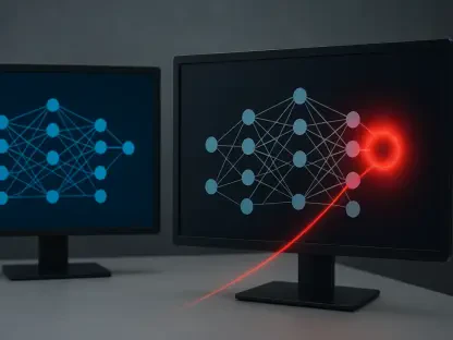

The current shift toward an all-optical data infrastructure is fundamentally transforming how artificial intelligence and cloud computing systems handle the massive throughput required for modern workloads. As integrated photonics moves from a specialized laboratory concept to a primary architectural foundation, the limitations of traditional electronic circuitry have become a significant bottleneck for global data centers. While light provides unparalleled transmission speed and reduced thermal output, managing the flow of photons on a microscopic scale presents a unique set of engineering hurdles that have historically slowed commercial adoption. One of the most persistent obstacles in this field has been the lack of a reliable, high-performance optical isolator that can be fabricated directly onto a semiconductor chip. Without a robust mechanism to ensure light travels in only one direction, sensitive laser sources are frequently compromised by back-reflections that cause noise, signal instability, or permanent physical damage to the hardware.
Historical Limitations: The Problem with Magnetic Materials
For decades, the standard solution for preventing harmful back-reflections has relied on the Faraday effect, which utilizes bulky magneto-optic materials and external magnetic fields to manipulate light polarization. Although highly effective in large-scale laboratory setups, these components are notoriously difficult to integrate into the streamlined manufacturing processes used for modern microchips. The specialized materials required for magnetic isolation, such as garnets, are fundamentally incompatible with standard silicon-based fabrication, leading to high production costs and significant signal loss during transmission. Furthermore, the presence of permanent magnets introduces unwanted electromagnetic interference and occupies a disproportionate amount of physical space, making them unsuitable for the high-density environments of modern computing. Engineers have faced a persistent trade-off between device protection and the necessity for miniaturization, leaving a critical gap in the architecture of next-generation optical networks.
In contrast to magnetic systems, previous attempts to bypass these dependencies often turned to acousto-optic methods, which use sound waves to create a non-reciprocal environment for light propagation. While these devices showed initial promise, they introduced a new set of mechanical vulnerabilities that limited their practical application in rugged industrial environments. These systems relied on physical vibrations that could be easily dampened or disrupted by standard protective coatings, requiring the components to remain exposed and fragile. Additionally, the tuning range of these sound-based isolators was often too narrow to accommodate the wide spectrum of wavelengths used in modern telecommunications, forcing designers to create highly specific hardware for each individual application. The search for a truly robust and scalable solution necessitated a move away from mechanical movement altogether, pushing researchers toward more sophisticated electrical control mechanisms that could be seamlessly protected within a chip’s package.
Electro-Optic Breakthrough: Harnessing Autler-Townes Splitting
A significant breakthrough has emerged from recent research efforts, where engineers successfully applied principles from atomic physics to the field of integrated photonics. By utilizing a phenomenon known as Autler-Townes splitting, a team at the University of Illinois Urbana-Champaign developed a method to break the symmetry of light propagation using electro-optic modulation on a lithium niobate platform. This design involves applying high-frequency electrical signals to create an energy barrier that selectively blocks light based on its direction of travel. In this configuration, photons moving in the intended forward direction pass through the system with minimal resistance, while those attempting to travel backward encounter a fragmented energy state that prevents their passage. This elegant solution effectively recreates the “one-way street” functionality of a magnetic isolator without requiring a single magnet, marking a fundamental shift in how engineers approach signal routing.
The choice of lithium niobate as the foundational material for this new isolator was intentional, as it offers exceptional electro-optic properties that are critical for high-speed modulation. Unlike earlier experimental designs, this electro-optic system contains no moving parts, making it far more durable and easier to manufacture at scale using existing semiconductor facilities. Because the isolation effect is controlled by electrical signals rather than physical vibrations, the entire device can be encapsulated in a standard protective layer without sacrificing performance. This encapsulation is vital for maintaining the longevity of the chip in the harsh thermal environments of high-power computing clusters. Moreover, the ability to electronically tune the isolation parameters allows the hardware to adapt to different laser frequencies on the fly, providing a level of flexibility that was previously unattainable with fixed-frequency magnetic or acoustic components.
Operational Excellence: Achieving Record-Breaking Isolation Ratios
In terms of raw performance, this new on-chip isolator has reached a level of efficiency that rivals, and in some cases exceeds, that of expensive commercial magnetic devices. Recent testing demonstrated an isolation ratio of 33 decibels, which translates to blocking more than 99.9% of all backward-traveling light that would otherwise interfere with the laser source. Maintaining such a high degree of isolation while ensuring the forward signal remains clear and uninhibited is a difficult balancing act that this new design handles with remarkable precision. This performance level is particularly impressive because it is achieved within a compact footprint that can be easily integrated alongside other optical components. For the first time, engineers have a non-magnetic tool that provides the necessary protection for high-power lasers without the bulk, cost, or manufacturing complexity that has long hindered the progress of complex photonic integrated circuits.
The development of a broadband version of this isolator represented a pivotal shift in the industry as researchers sought to manage multiple wavelengths without constant active tuning. This work, supported by major research agencies, demonstrated that an all-optical future was finally within reach for the global computing market. These advancements showcased a clear path for systems to handle massive data loads with a level of speed and energy efficiency that traditional electronics never matched. By prioritizing these scalable on-chip components, the engineering community successfully established a new standard for high-density photonic integration. This breakthrough solidified the role of lithium niobate as a primary material for future-proofing networks against the rising power requirements of artificial intelligence. Consequently, the transition toward fully integrated light-based routing transitioned from a theoretical goal to a practical reality for the next decade.