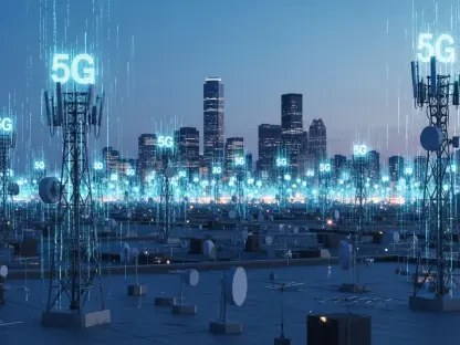

The deployment of 6G wireless technology has fundamentally transformed our digital landscape by offering terabit-per-second speeds, yet this advancement faces a significant physical wall where high-frequency signals fail to penetrate the very materials that define our modern urban environments. While current 5G networks utilize lower frequencies that can navigate around structures with relative ease, the move toward sub-terahertz bands introduces a reality where even a single sheet of glass or a cluster of moving pedestrians can completely disrupt the connection flow. This propagation sensitivity creates a frustrating paradox where the fastest possible internet is only available in direct line-of-sight conditions, leaving indoor spaces and dense city corridors in a state of digital isolation. To address this, researchers have pivoted away from power-hungry electronics toward passive materials that can literally sculpt the path of radio waves. By utilizing 3D-printed metacrystal panels, engineers found a way to bridge these coverage gaps without adding to the energy burden of the global network infrastructure.
The Limitations of Conventional 6G Infrastructure
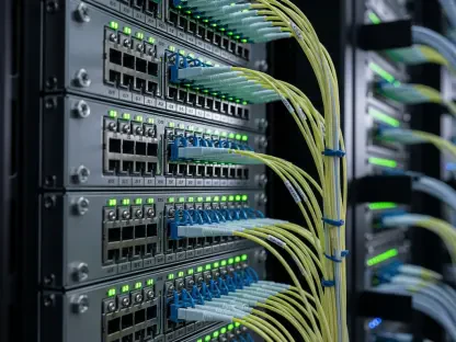
Challenges: The High Cost and Complexity of Active Hardware
Expanding network coverage for high-frequency bands traditionally requires the installation of active electronic components such as small cells, repeaters, or massive MIMO antenna arrays. These devices are remarkably effective but come with a heavy price tag that makes wide-scale deployment a logistical and financial nightmare for many telecommunications providers. Beyond the initial purchase price of the hardware, the sheer quantity of units needed to blanket a single metropolitan area leads to a ballooning of capital expenditure that often outweighs the immediate revenue benefits of the upgraded service. Furthermore, every active node requires a dedicated power source, which complicates installation in older buildings or outdoor public spaces where wiring is not readily available. This constant demand for electricity also places a significant strain on municipal power grids and contradicts the increasing global push for carbon-neutral technological solutions. As the number of connected devices continues to rise, the energy consumption of these active sites becomes an unsustainable operational cost.
Constraints: Reliability and Maintenance in Demanding Environments
Active electronic hardware is inherently susceptible to environmental degradation and mechanical failure, necessitating a rigorous and expensive maintenance schedule that many operators struggle to maintain. In specialized environments such as subway tunnels, industrial basements, or expansive manufacturing facilities, the physical conditions are often too harsh for sensitive microchips and cooling fans to operate reliably over long periods. Dust, humidity, and temperature fluctuations can lead to frequent hardware malfunctions, requiring technicians to manually service or replace components in difficult-to-reach locations. This reliance on delicate circuitry creates a fragile ecosystem where a single equipment failure can lead to significant connectivity blackouts for end-users. Additionally, active hardware often requires periodic software updates and cybersecurity patches to remain functional and secure, adding another layer of complexity to the overall management of the network. Because of these persistent vulnerabilities, there is a growing consensus that the next generation of connectivity must rely on more resilient, low-maintenance physical solutions.
The Science Behind Metacrystal Innovation
Engineering: The Role of Inverse Design and Additive Manufacturing
The breakthrough in managing high-frequency signal propagation came from the development of metacrystals, which are artificially engineered materials designed to interact with electromagnetic waves in ways that natural substances cannot. Researchers at Aalto University utilized advanced inverse-design algorithms to determine the precise internal geometry required to steer or focus radio waves around specific obstacles. Instead of starting with a known shape and testing its properties, this mathematical approach starts with the desired outcome—such as a specific signal redirection angle—and calculates the exact volumetric structure needed to achieve it. Once the design is finalized, the resulting complex architecture is produced using standard industrial 3D printers and inexpensive thermoplastic materials. This method allows for the creation of intricate internal patterns that would be impossible to manufacture using traditional molding or milling techniques. Because these structures are crafted from basic plastics, the manufacturing process is both scalable and highly cost-effective, providing a path for mass production that meets the demands of rapid urban expansion.
Mechanics: Advanced Wave Manipulation Through Volumetric Design
While previous attempts at signal management relied on two-dimensional intelligent reflecting surfaces, these newer 3D metacrystals offer a much higher degree of control over the electromagnetic environment. These volumetric structures do not simply reflect a wave like a mirror; they can be engineered to filter, refract, or even absorb specific frequencies based on their internal arrangement. This allows engineers to manage multiple signals simultaneously, ensuring that high-speed data streams are directed toward users while interfering noise is suppressed. The three-dimensional nature of the crystals provides more surface area and complex paths for the waves to travel, which enables the manipulation of the signal phase and amplitude with extreme precision. This versatility is crucial for the sub-terahertz frequencies used in 6G, which behave more like light than traditional radio waves and are easily blocked by common architectural features. By strategically placing these panels, network designers can effectively “clean” the signal landscape, turning dead zones into high-connectivity hubs. This level of environmental sculpting represents a paradigm shift from trying to force signals through walls to gently guiding them around.
Practical Applications and Future Sustainability
Deployment: Scaling Low-Cost Solutions for Smart Urban Areas
One of the most compelling aspects of the 3D-printed metacrystal approach is the dramatic reduction in cost, with individual panels often costing only a few dozen euros to manufacture at scale. This affordability enables telecommunications companies and municipal governments to deploy thousands of these units across a city without the massive financial risk associated with active electronics. Because these panels are entirely passive and require no electricity, they represent a truly sustainable “green” technology that aligns with global initiatives to reduce the carbon footprint of digital infrastructure. They can be integrated into the existing urban landscape with minimal aesthetic impact, serving as hidden enhancers for the smart city services of the present. From powering autonomous vehicle navigation at busy intersections to ensuring seamless data transfer for wearable health monitors, these panels provide the backbone for a ubiquitous connectivity layer. By minimizing the reliance on high-power antennas, the technology also reduces the overall electromagnetic noise in a city, creating a more efficient and cleaner spectrum for all wireless users to share.
Evolution: Toward Reconfigurable and Integrated Architectural Elements
The potential for these panels extends beyond mere signal redirection, as researchers are already looking into ways to weave these structures directly into the materials used in modern construction. Future office buildings and residential complexes could feature metacrystal technology embedded within drywall, ceiling tiles, or even window glass to ensure that every corner of a room receives a perfect signal. In industrial settings, these panels are becoming essential for maintaining the connectivity of autonomous robotic fleets that navigate through metal-heavy warehouses where signals are notoriously unstable. While current iterations of the technology are fixed in their design, the next phase of development focuses on creating reconfigurable metacrystals that can adapt to environmental changes. These advanced versions would allow for the signal path to be adjusted if a new wall is built or if the layout of a factory floor is rearranged. This evolution transforms the physical environment from a series of obstacles into an active and helpful participant in the communication process. Such a transition ensures that the promise of 6G remains a reality for everyone, regardless of their location.
Long-Term Outlook for Wireless Infrastructure
Strategic Standards: Establishing Global Protocols for Passive Networks
To fully capitalize on the benefits of metacrystal technology, the telecommunications industry has begun to develop standardized protocols that integrate passive signal management into the broader network architecture. This strategic shift means that network planning is no longer just about where to place towers, but also about how the surrounding physical environment can be optimized for wave propagation. Regulatory bodies and engineering firms are collaborating to create guidelines for “signal-friendly” construction, encouraging the use of metacrystal-infused materials in new developments. These standards ensure that as 6G networks expand, the infrastructure is inherently designed to minimize dead zones and maximize spectral efficiency. Furthermore, this standardization allows for a more interoperable ecosystem where panels from different manufacturers can work in harmony within a single urban grid. By codifying these practices, the industry provides a clear roadmap for developers to follow, ensuring that connectivity becomes a built-in feature of the modern city. This move toward integrated passive infrastructure marks the beginning of a more reliable and cohesive global data network.
Future Directions: Orchestrating the Next Era of Wireless Communication
The introduction of 3D-printed metacrystal panels provided a definitive answer to the signal blockage challenges that once threatened the viability of ultra-high-speed 6G networks. By moving away from a reliance on expensive, power-hungry active hardware, researchers established a more resilient and sustainable framework for global connectivity. These passive structures demonstrated that the physical environment did not have to be an adversary to wireless signals but could instead be engineered to facilitate them. Looking ahead, the focus shifted toward the mass integration of these structures into standard building materials and urban furniture, effectively turning cities into intelligent conduits for data. This approach encouraged a new wave of architectural standards where signal propagation was considered as fundamental as plumbing or electricity during the initial design phase. As these solutions became more widespread, the digital divide caused by physical barriers largely vanished, paving the way for a more inclusive and reliable era of high-speed communication. The transition to this hybrid model of active transmitters and passive guides ensured that network performance remained robust in even the most complex environments.