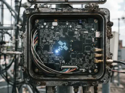

The unprecedented demand for generative artificial intelligence and massive computational models is currently pushing modern hardware to its absolute physical and thermal limits. As the complexity of neural networks grows at an exponential rate, traditional silicon-based electronics are struggling to keep pace, primarily due to the inherent constraints of electron-based data movement. Electricity moving through copper traces generates significant heat and is restricted by resistance, which ultimately caps the maximum data transmission speeds and inflates power consumption to unsustainable levels. As we move from 2026 toward a future defined by even larger models, the industry is approaching a technological wall where simply shrinking transistors is no longer a viable path for progress. Consequently, optical computing has emerged as a frontrunner to replace or augment current systems, utilizing photons rather than electrons to carry information. While the potential for light-speed processing and near-zero heat generation is immense, the volatile nature of light—which moves at a constant, blistering speed and lacks an inherent storage mechanism—has historically made it difficult to create the buffers and memory needed for practical computing.
A Breakthrough in On-Demand Light Control
Reconfiguring the Speed: The New Temporal Buffer
A collaborative research initiative involving teams from Seoul National University and the University of Seoul recently achieved a definitive milestone by engineering a programmable photonic integrated circuit capable of slowing down and controlling light with extreme precision. This innovation addresses one of the most persistent bottlenecks in optical engineering: the inability to manipulate the temporal characteristics of a signal once it has been launched into a chip. In legacy optical systems, the path and speed of light were determined during the manufacturing process, leaving no room for adjustment if data traffic patterns changed or if synchronization required a slight delay. The newly developed chip introduces a dynamic architecture where researchers can adjust the speed of light on demand, creating a functional “buffer” that allows for the orderly management of high-speed data packets within an AI-driven environment. By providing this level of control, the researchers have essentially turned a static physical medium into a flexible, software-defined resource that can adapt to the unpredictable timing requirements of modern data centers.
The implications of being able to shape and slow optical signals in real-time extend far beyond basic data transmission, as they provide the foundation for true optical memory. Since photons do not naturally stay in one place, the ability to delay them within a microchip effectively allows the system to “hold” information for a calculated period, which is a critical requirement for any computational logic. This breakthrough, which was detailed in recent scientific publications, demonstrates that light can be harnessed to perform complex operations that were previously reserved for electronic components. By integrating these programmable buffer functions directly into the photonic hardware, the design minimizes the need for cumbersome conversions between light and electricity. This transition not only preserves the integrity of the data but also ensures that the high-bandwidth benefits of photonics are not lost to the latency of traditional electronic processing units. The result is a highly efficient architecture that can serve as the backbone for next-generation AI accelerators.
Bridging the Gap: Overcoming Photon Volatility
The fundamental challenge with utilizing light for computation has always been its relentless velocity and the lack of a natural “pause” button, which is why this new programmable chip is considered a game-changer. In electronic circuits, capacitors and transistors can easily store a charge to represent a bit of data, but a photon must be kept in motion or absorbed. To solve this, the Seoul-based researchers designed a system that uses internal loops and resonators to trap and circulate light, effectively creating a holding pattern that acts as a bridge between different processing stages. This method allows the chip to synchronize various data streams that might be arriving from different parts of a global network at slightly different times. Without this synchronization, the high-speed data would collide or be lost, making coherent AI processing impossible at the scale required for contemporary large language models and real-time inference engines.
This newly established bridge between volatile light and stable computation is particularly vital for the future of decentralized AI and edge computing. In these scenarios, signals from thousands of sensors or remote servers must be aligned perfectly to be processed by a central unit. The ability of the photonic chip to act as a programmable delay line means that engineers can now fine-tune the arrival of each packet of information with femtosecond precision. This eliminates the “jitter” and timing errors that often plague high-speed telecommunications, allowing for a much cleaner and more reliable signal. Furthermore, because this delay is programmable through software, the hardware does not need to be replaced as the network evolves or as the software protocols become more demanding. The agility provided by this technology ensures that optical computing can finally move out of the laboratory and into the rigorous, fast-paced world of industrial data centers and global communication hubs.
The Shift from Static to Programmable Hardware
Redefining Resonator Interference: From Static to Dynamic
The scientific principle enabling this level of control is known as Coupled-Resonator-Induced Transparency, or CRIT, which manipulates how light waves interfere with one another inside tiny circular structures called resonators. In the past, devices utilizing CRIT were built with a fixed geometry, meaning the frequency and the delay they provided were hard-coded into the physical material at the time of fabrication. If a data center operator needed a different delay to accommodate a new type of AI workload, they would have had to manufacture an entirely different chip, which was both cost-prohibitive and incredibly slow. The research team from South Korea overcame this limitation by introducing controllable loop couplers into the resonator design, allowing the interference patterns to be adjusted after the chip is already in use. This shift from static to dynamic hardware represents a fundamental change in photonic design, where the physical properties of the chip are no longer permanent but are instead a set of parameters that can be optimized on the fly.
By treating the different optical states within these resonators as a single, unified degree of freedom, the researchers simplified the control mechanism required to program the chip. Instead of needing thousands of independent adjustments, the system can be reconfigured by changing a few key variables, which significantly reduces the complexity of the control software. This allows the chip to transition between being a high-speed transmission line and a high-capacity temporal buffer in a matter of microseconds. This flexibility is essential for AI tasks that vary in intensity, such as moving from a low-power “sleep” state to a high-intensity “training” state. The ability to program the hardware post-fabrication also drastically lowers the barrier to entry for smaller tech firms, as they can use a standardized photonic chip and customize its performance via software to meet their specific needs, rather than investing millions in custom hardware development.
Operational Flexibility: Adapting to Real-Time Demands
The versatility of this programmable architecture is most evident when considering the fluctuating bandwidth requirements of modern cloud services. Current static optical chips are often over-engineered to handle peak loads, which leads to significant inefficiencies during periods of lower activity. In contrast, the programmable photonic circuit can tighten or widen its bandwidth and adjust its signal delay based on the actual real-time traffic it is receiving. This operational flexibility allows for a much more efficient use of the available light spectrum, maximizing the amount of data that can be sent through a single fiber-optic strand. As AI models become more distributed, with parts of the network running on different servers across the globe, the ability to dynamically manage the flow of information becomes a critical factor in maintaining system-wide performance and reducing the latency that users experience.
Moreover, the software-defined nature of these chips allows for a level of error correction that was previously unattainable in optical systems. If a specific part of the chip experiences a slight thermal drift or a minor manufacturing defect, the control software can compensate by recalibrating the resonators to maintain the desired output. This self-healing capability is essential for large-scale deployments where manual maintenance of thousands of individual chips would be impossible. By providing a hardware platform that can be tuned and optimized via code, the researchers have paved the way for a more resilient and adaptable computational infrastructure. This technology essentially brings the flexibility of a field-programmable gate array (FPGA) to the world of photonics, combining the raw speed of light with the sophisticated control of modern digital logic, which is exactly what the next decade of AI development will require.
Reliability and Industrial Versatility
Testing Performance: Durability in Hostile Environments
For any new hardware technology to succeed in the competitive world of data centers, it must prove that it can operate reliably under the stressful conditions of a real-world environment. The Seoul research team addressed this concern by utilizing silicon nitride as the primary material for their photonic circuits, a choice that offers several distinct advantages over standard silicon. Silicon nitride is known for its exceptional thermal stability and its ability to handle high-power optical signals without degrading or losing clarity. During rigorous simulations and laboratory testing, the chip demonstrated that it could maintain its programmed states even when subjected to significant heat interference from nearby electronic components. This is a crucial finding, as data centers are notoriously hot environments where temperature fluctuations can easily disrupt the delicate balance of an optical signal, leading to data loss or system crashes.
Beyond thermal stability, the researchers focused on the chip’s ability to resist “crosstalk,” which occurs when signals from adjacent paths interfere with one another. In high-density chips, where thousands of optical paths are packed into a tiny area, preventing this interference is one of the most difficult engineering challenges. The programmable nature of the new circuit allows it to actively tune its internal filters to block out noise and maintain a high signal-to-noise ratio. This level of durability ensures that the technology is not just a laboratory curiosity but a robust solution ready for industrial scaling. The success of these tests indicates that photonic chips can finally match the reliability of their electronic counterparts, providing a stable foundation for the mission-critical applications that define the modern digital economy, from financial high-frequency trading to emergency response coordination.
Seamless Integration: Synchronizing High-Speed Networks
The ability to control light in real-time opens up new possibilities for the seamless integration of diverse network components, acting as a universal translator for different optical wavelengths. In current infrastructures, converting a signal from one frequency to another often requires bulky and expensive equipment that adds significant latency and power consumption. The programmable photonic chip, however, can perform frequency conversion and signal synchronization internally by adjusting the resonance properties of its circuits. This allows it to act as a high-speed “traffic controller” at the junction of different networks, ensuring that data packets from various sources are perfectly aligned and formatted before they reach the main processing units. This capability is particularly important for the deployment of 6G communications, where the sheer volume and speed of data will require an unprecedented level of synchronization.
Furthermore, the integration of these chips into existing data center architectures is made easier by their compatibility with standard manufacturing processes. Because they are built using materials and techniques that are already common in the semiconductor industry, they can be produced at scale using existing fabrication facilities. This ease of integration means that the transition from electronic-heavy systems to photon-enhanced systems can happen incrementally, allowing companies to upgrade their infrastructure without needing to replace every single component at once. The chip effectively serves as a bridge between the legacy world of electrons and the future world of photons, providing a clear and attainable roadmap for the evolution of global computing networks. By eliminating the need for extra hardware to manage signal timing and frequency, these programmable circuits simplify the overall system architecture, leading to lower costs and higher overall reliability.
Reshaping the Global Technological Landscape
Expanding the Reach: Photonic Applications Beyond AI
While the primary driver for programmable photonic chips is the need for faster AI processing, the versatility of this technology ensures that its impact will be felt across many other sectors, including autonomous transportation. Self-driving vehicles rely on Lidar and a suite of sensors to create a real-time map of their surroundings, a task that requires processing vast amounts of data with zero perceptible delay. The ability of photonic circuits to handle these data streams at the speed of light—without the heat-related throttling seen in traditional processors—could significantly enhance the safety and responsiveness of autonomous systems. In a high-stakes environment where a millisecond of delay can be the difference between a safe stop and a collision, the low-latency processing provided by these programmable chips offers a level of performance that electronic chips simply cannot match.
In the specialized field of quantum computing, the ability to precisely manipulate individual photons is a fundamental requirement for the development of quantum memory and advanced logic gates. The programmable resonators developed by the Seoul research team provide a platform for controlling the quantum states of light with the high degree of accuracy needed for quantum information processing. By allowing researchers to “pause” and “store” quantum bits, or qubits, within a photonic circuit, this technology brings us closer to the realization of a functional quantum internet. This overlap between AI computing and quantum research highlights the broad utility of programmable photonics, suggesting that the same hardware used to speed up a large language model could also be the key to unlocking the next generation of cryptographic security and scientific discovery.
Sustainable Infrastructure: Efficiency in the 6G Era
The global transition toward a light-based computing standard represented a critical move for achieving environmental sustainability in a world increasingly dominated by power-hungry data centers. Industry leaders recognized that the massive carbon footprint associated with cooling traditional electronic hardware was no longer acceptable, prompting a pivot toward the energy-efficient properties of programmable photonic circuits. By reducing the frequent and energy-intensive conversions between optical and electronic signals, these chips allowed for a much leaner architecture that consumed a fraction of the power required by legacy systems. This shift proved essential as the world moved into the 6G era, where the volume of data being processed reached levels that would have overwhelmed the global energy grid if left to traditional silicon-based processors.
Stakeholders realized the long-term value of investing in “software-defined light” to meet the evolving demands of cloud infrastructure and edge computing. The research conducted by the teams in Seoul established a new benchmark for what was possible in optical engineering, proving that light could be controlled with the same level of granularity as electricity. As a result, the industry adopted these programmable architectures to solve the immediate bottlenecks of signal synchronization and thermal management in large-scale AI deployments. The successful implementation of these chips demonstrated that the physical boundaries of Moore’s Law did not mark the end of progress, but rather the beginning of a more efficient and capable era of computing. This transition ensured that the continued growth of artificial intelligence remained both technologically feasible and environmentally responsible, setting the stage for decades of sustainable innovation.