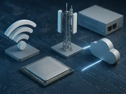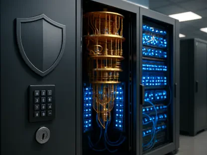

The relentless advancement of Artificial Intelligence is generating an unprecedented data deluge that threatens to overwhelm the very physical infrastructure designed to support it, creating a critical chokepoint in the heart of modern data centers. As AI models scale exponentially, the demand for faster, denser communication between processors is pushing traditional copper wiring to its absolute physical limits. This looming “copper bottleneck” is no longer a distant theoretical problem but an immediate barrier that could stall progress in high-performance computing. The industry finds itself at a crossroads, with legacy copper interconnects faltering under the strain and their primary alternative, optical fiber, proving to be an imperfect substitute for the unique demands of tightly integrated systems. This has ignited an urgent search for a third way—a disruptive technology capable of bridging the widening gap and ensuring that the physical links between chips can keep pace with the voracious computational appetite of next-generation AI.
The Imminent Failure of Incumbent Interconnects
The challenge is most acute in the domain of “scaling up” AI systems, which involves packing an ever-increasing number of Graphics Processing Units (GPUs) into a single, cohesive super-processor. This requires extremely fast, dense, and short-range connections, a realm where copper has long been the cost-effective standard. However, as GPU-to-GPU data rates push toward the terabit-per-second realm, engineers are confronting a hard physical limit known as the “copper cliff.” At the high frequencies needed for such speeds, a phenomenon called the “skin effect” forces the electrical current to flow only along the outer surface of the wire. This effectively shrinks the conductor’s usable area, which in turn dramatically increases electrical resistance. To overcome this, the only solutions are to make copper wires thicker and shorter, while also pumping more power through them to drive the signal. This approach is becoming physically and economically unsustainable in already congested computer racks, especially as industry roadmaps call for an eightfold increase in maximum GPU density per system by 2027. While stopgap measures like Active Electrical Cables (AECs), which use special chips to regenerate the signal, can extend copper’s reach, they are a temporary fix that adds its own complexity, cost, and power consumption to an already strained system.
While optical fiber has become the undisputed champion for “scaling out” by connecting systems over long distances across data centers, it presents its own significant set of drawbacks when applied to the dense, short-range environment of a scale-up architecture. Photonics systems are notoriously power-hungry, with estimates suggesting they consume around 10% of a data center’s entire compute budget. This inefficiency is a major concern in an industry where energy consumption is a primary operational cost and environmental consideration. Furthermore, optical components are highly sensitive to temperature fluctuations, which can degrade performance and lead to long-term reliability issues, a problem colloquially known as “link flap.” Perhaps the most significant barrier is the sheer complexity and cost of manufacturing. Aligning the microscopic core of an optical fiber with the waveguide on a photonic chip requires micrometer-level precision, a process that is difficult to scale and unforgiving of even the slightest error. This combination of high power draw, questionable long-term stability, and extreme manufacturing difficulty makes optics a less-than-ideal solution for replacing copper in the dense, high-stakes environment inside an AI server.
A Radio-Frequency Paradigm Shift
This technological gap between the limitations of copper and the impracticalities of short-range optics has created a fertile ground for a new class of interconnect based on radio frequencies. This innovative approach involves converting digital data into modulated RF signals, typically in the millimeter-wave or terahertz spectrum, and transmitting them through a specialized, non-copper waveguide. This paradigm promises to deliver the low cost, manufacturing ease, and reliability of traditional electronics-based systems while achieving performance characteristics—such as longer reach, lower power consumption, and a much thinner cable profile—that are more akin to optical fiber. Two pioneering startups, Point2 Technology and AttoTude, are at the forefront of this movement, championing a solution that could fundamentally alter the economics and design of AI hardware. Their technology offers a practical path forward, avoiding the physical cliff of copper and the complex, costly ecosystem of photonics.
Point2 Technology is already making significant commercial headway, backed by industry manufacturing giants like Molex and Foxconn. The company’s flagship product, the “Active Radio Cable” (ARC), is built from multiple individual “e-Tube” fibers, each a slender polymer waveguide with a metal cladding. At each end, a standard silicon chip handles the conversion between digital bits and the modulated RF signals. A 1.6 Tb/s ARC cable, operating at millimeter-wave frequencies, boasts half the volume of a comparable copper AEC and offers up to 20 times the reach. Against optical solutions, Point2 claims its system consumes one-third the power at one-third the cost, with latency that is orders of magnitude lower. A critical element of its commercial viability is the ability to fabricate the necessary chips using mature, inexpensive 28-nanometer CMOS technology. This sidesteps the need for cutting-edge, costly fabrication plants and allows the waveguides themselves to be manufactured on existing production lines, ensuring the solution is both scalable and cost-effective from day one.
Redefining the Future of AI Hardware
The implications of this emerging RF technology extended far beyond a simple one-for-one cable replacement, promising to reshape the very architecture of data centers. The current reliance on short, passive copper cables forces system designers to pack GPUs into extremely dense configurations to minimize connection lengths. This high density, in turn, creates immense thermal challenges that necessitate the use of complex and expensive liquid cooling systems to prevent overheating. The significantly longer reach afforded by RF cables—up to 20 meters in some designs—would liberate engineers from these constraints. It would allow GPUs and other processors to be spaced further apart, creating a “disaggregated” system architecture that simplifies cooling, improves serviceability, and potentially reduces the overall physical footprint and operational cost of AI infrastructure. This newfound design freedom could ease one of the most significant engineering hurdles currently facing the industry.
The most profound and transformative vision for this technology centered on the concept of co-packaging, which involved integrating the RF transceivers directly into the same package as the GPU itself. This approach represented the ultimate in efficiency, eliminating centimeters or even meters of external cabling and the associated signal loss, latency, and power consumption. While industry leaders had been actively pursuing co-packaged optics to achieve this goal, they faced immense manufacturing challenges related to the precise, sub-micron alignment of optical fibers. RF technology, however, held a decisive and inherent advantage. The much longer wavelengths of millimeter-wave and terahertz signals relaxed the required alignment tolerance from the microscopic scale to a level so manageable that it could be demonstrated by hand. This dramatic simplification in manufacturing made co-packaged RF a more practical, reliable, and ultimately more manufacturable long-term solution, positioning it as the potential cornerstone for the next generation of integrated, high-performance AI systems.