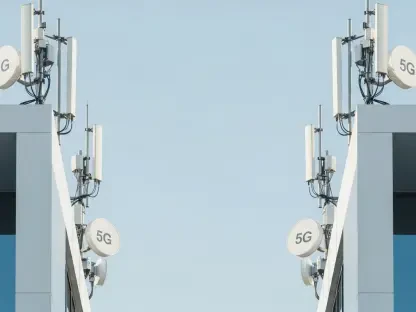

In an era where the Internet of Things (IoT) is reshaping daily life with billions of connected devices, the demand for efficient, low-power chip solutions has never been more critical. VeriSilicon, a leading semiconductor company listed on the Shanghai Stock Exchange (688521.SH), has stepped up to this challenge with the unveiling of a groundbreaking wireless IP platform on September 24 in Shanghai. Built on GlobalFoundries’ advanced 22FDX® (22nm Fully Depleted Silicon-On-Insulator) process technology, this platform is poised to transform chip design for IoT and consumer electronics markets. It offers a comprehensive suite of intellectual property (IP) solutions designed to enhance wireless connectivity across a spectrum of standards and distances. From short-range Bluetooth Low Energy (BLE) to long-range cellular options, the technology addresses the pressing need for energy-efficient, high-performance chips. This innovation not only reflects VeriSilicon’s commitment to tackling modern connectivity challenges but also sets a new benchmark for integration and power optimization in the industry.
Exploring the Technological Backbone
Unpacking the 22FDX® FD-SOI Process
The foundation of VeriSilicon’s latest wireless IP platform lies in GlobalFoundries’ 22FDX® FD-SOI process technology, a cutting-edge approach that prioritizes ultra-low power consumption and high integration. This 22nm process is specifically engineered to minimize leakage current, a common issue in battery-powered devices, thereby extending operational life without compromising performance. The FD-SOI architecture allows for exceptional transistor control, enabling chips to operate efficiently across various power modes. This is particularly beneficial for IoT applications where devices often switch between active and sleep states. By leveraging this technology, VeriSilicon ensures that its platform can support a diverse array of wireless standards, including Bluetooth Low Energy (BLE), Narrowband IoT (NB-IoT), and Global Navigation Satellite System (GNSS). The result is a robust framework that meets the stringent demands of modern connected devices, paving the way for smaller, more efficient chips that don’t sacrifice capability.
A deeper look into the 22FDX® process reveals its adaptability to multiple connectivity needs, from short-range to long-range communications. This flexibility is crucial in a landscape where IoT devices must seamlessly interact across different protocols, such as cellular Cat.1 and Cat.4 for broader network coverage. The technology’s inherent ability to integrate complex functionalities into a compact form factor also reduces the overall area required for chip design, optimizing the power, performance, and area (PPA) metrics. For manufacturers, this translates to cost savings and faster development cycles. Additionally, the process supports high-frequency operations needed for advanced wireless standards, ensuring that VeriSilicon’s platform remains future-proof as connectivity requirements evolve. This technological synergy underscores a significant step forward in addressing the energy constraints that have long plagued IoT hardware, offering a scalable solution for a wide range of consumer and industrial applications.
Innovations Driving Efficiency
One of the standout features of VeriSilicon’s platform is the integration of Adaptive Body Biasing (ABB) technology, a sophisticated method to enhance power efficiency in chip operation. ABB dynamically adjusts the voltage applied to transistors based on workload, significantly reducing power consumption during low-activity periods while maintaining performance during peak demands. This innovation is particularly impactful for battery-dependent IoT devices, where extending usage time between charges is a top priority. By fine-tuning power usage at the hardware level, VeriSilicon addresses a critical pain point in device design, ensuring that end-users experience longer-lasting products. This approach not only improves user satisfaction but also aligns with global sustainability goals by reducing energy waste in countless connected devices deployed worldwide.
Beyond ABB, the platform offers a comprehensive IP portfolio that includes radio frequency (RF) components, baseband processing, and software protocol stacks. This all-in-one solution streamlines the chip design process by providing pre-verified, silicon-proven elements that reduce development risks and accelerate time-to-market. Designers can access a complete set of tools to build chips supporting multiple wireless standards without starting from scratch, a significant advantage in a competitive market. The inclusion of software stacks ensures seamless integration between hardware and application layers, simplifying the creation of complex systems like smart home hubs or wearable health monitors. This holistic approach reflects a deep understanding of the challenges faced by chip designers, offering a practical pathway to innovation while maintaining high standards of performance and reliability across diverse use cases.
Market Reach and Strategic Alliances
Demonstrating Real-World Success
VeriSilicon’s wireless IP platform has already made a substantial impact on the market, with over 100 million chips shipped based on its designs. This impressive figure highlights the technology’s reliability and widespread acceptance across various sectors, particularly in IoT and consumer electronics. Real-world applications are diverse, ranging from low-power BLE microcontrollers (MCUs) used in wearable fitness trackers to Wi-Fi 802.11ah-enabled home security cameras that provide long-range, energy-efficient connectivity. These examples showcase the platform’s versatility in meeting specific needs, whether it’s enabling compact, battery-conscious designs for personal gadgets or supporting robust systems for smart home ecosystems. The sheer volume of deployed chips serves as a testament to the trust manufacturers place in VeriSilicon’s solutions, affirming the platform’s role as a cornerstone for modern connected device development.
Further examination of these applications reveals the platform’s ability to cater to niche markets while maintaining broad appeal. For instance, high-precision GNSS System-on-Chips (SoCs) powered by this technology are integral to navigation systems in automotive and logistics industries, where accuracy and low power are non-negotiable. Similarly, the adoption in smart home devices underscores how the platform supports emerging trends like home automation, where devices must communicate over extended periods without frequent recharging. This adaptability across different product categories not only demonstrates technical prowess but also highlights market responsiveness. By addressing varied consumer demands—from personal tech to industrial solutions—VeriSilicon has positioned its platform as a go-to resource for companies aiming to innovate quickly and efficiently in a fast-paced digital landscape.
Power of Industry Partnerships
A pivotal element of VeriSilicon’s success with this platform is its strategic collaboration with GlobalFoundries, a partnership that amplifies the capabilities of both entities. The 22FDX® process technology, central to the platform’s performance, benefits from GlobalFoundries’ expertise in advanced manufacturing, ensuring that the chips meet stringent quality and efficiency standards. Endorsements from industry leaders, such as senior executives at GlobalFoundries, emphasize the synergy between VeriSilicon’s IP design prowess and cutting-edge fabrication techniques. This alliance enables the delivery of market-ready solutions that combine innovative design with reliable production, a critical factor in gaining customer confidence. Such collaborations are increasingly vital in the semiconductor space, where complex challenges require integrated expertise to push technological boundaries.
This partnership also reflects a broader industry trend toward collaborative innovation, where IP providers and foundries work hand-in-hand to address market needs. By aligning their strengths, VeriSilicon and GlobalFoundries have created a platform that not only meets current demands but also anticipates future requirements, such as higher integration for next-generation devices. The shared vision of accelerating innovation across multiple markets—from consumer electronics to automotive applications—underscores the strategic importance of this relationship. It ensures that customers receive solutions that are not just theoretical but proven in mass production, reducing the risks associated with adopting new technologies. This model of cooperation sets a precedent for how industry alliances can drive progress, offering a blueprint for tackling the evolving complexities of wireless connectivity in an interconnected world.
Vision for Tomorrow’s Connectivity
Pioneering New Frontiers
Looking ahead, VeriSilicon is committed to exploring emerging opportunities with its wireless IP platform, targeting cutting-edge areas like Wi-Fi 6, satellite communications, and millimeter-wave radar. These fields represent the next wave of connectivity, promising faster data rates, broader coverage, and enhanced precision for applications ranging from smart cities to autonomous vehicles. The company’s vision also extends to specialized sectors such as smart glasses and hearing aids, where compact, low-power chips are essential for user comfort and functionality. With a robust track record of licensing over 300 FD-SOI IPs to 45 customers and supporting mass production across diverse industries, VeriSilicon is well-equipped to lead in these innovative domains. This forward-looking approach ensures that the platform remains relevant as technology landscapes shift, addressing both current and anticipated needs with agility and expertise.
The focus on satellite communications, in particular, highlights VeriSilicon’s ambition to redefine long-range connectivity, a critical component for global IoT networks. Similarly, advancements in Wi-Fi 6 aim to support the increasing bandwidth demands of modern devices, ensuring seamless performance in crowded network environments. The exploration of millimeter-wave radar technology also opens doors to high-resolution sensing applications, vital for automotive safety systems. These initiatives are underpinned by the company’s extensive experience, evidenced by customized FD-SOI chips for 43 customers and 33 designs in mass production. By investing in these areas, VeriSilicon not only anticipates market evolution but also shapes it, offering solutions that empower manufacturers to stay ahead of the curve in creating next-generation products that redefine how connectivity integrates into everyday life.
Meeting the Pulse of Industry Demands
The wireless IP platform is strategically aligned with the growing demand for low-power, multi-standard connectivity solutions in the IoT ecosystem, where billions of devices require efficient communication without draining resources. Energy efficiency remains a top concern as devices proliferate in homes, industries, and public spaces, necessitating chips that can handle multiple protocols like BLE, NB-IoT, and cellular standards within tight power budgets. VeriSilicon’s technology addresses this by optimizing PPA metrics, ensuring that devices operate longer on minimal energy while supporting complex interactions. This capability is crucial for sustaining the rapid expansion of connected ecosystems, where reliability and battery life directly impact user adoption and satisfaction in an increasingly digital world.
Moreover, the platform mirrors broader industry trends toward integrated, turnkey solutions that simplify chip design complexities. By offering a unified set of IPs encompassing RF components, baseband processing, and software stacks, VeriSilicon reduces the burden on designers to piece together disparate elements, allowing them to focus on product differentiation. This trend toward consolidation is evident as manufacturers seek faster, more cost-effective ways to bring products to market amid rising competition. The platform’s ability to support diverse applications—from wearables to smart infrastructure—positions it as a vital tool in meeting these market needs. As IoT continues to evolve, such solutions will play a pivotal role in enabling scalable, energy-conscious designs that underpin the future of connectivity, reflecting a shift toward smarter, more sustainable technological frameworks.
Reflecting on a Milestone Achievement
Reflecting on VeriSilicon’s launch of the FD-SOI wireless IP platform, it’s clear that this development marked a significant stride in addressing the intricate demands of IoT and consumer electronics chip design. The collaboration with GlobalFoundries to harness the 22FDX® process technology delivered a solution that balanced ultra-low power with high performance, setting a new standard for connectivity. With over 100 million chips shipped and applications spanning wearables to smart home systems, the platform proved its reliability and market fit. Looking ahead, the focus should shift to scaling these innovations into emerging fields like satellite communications and Wi-Fi 6, ensuring that the technology continues to evolve with industry needs. Stakeholders are encouraged to explore how such platforms can be adapted for specific challenges, fostering partnerships that drive further advancements. This milestone serves as a foundation for tackling future connectivity hurdles with practical, forward-thinking strategies.