
The physical limits of copper wiring are finally colliding with the voracious data demands of modern artificial intelligence, forcing a radical shift toward light-based communication. As Large Language Models grow exponentially, the electrical resistance found in traditional metal traces has become a literal heat sink that drains efficiency and throttles performance. Optical interconnect technology addresses this by replacing electrons with photons, utilizing Photonic Integrated Circuits to move data at speeds that were previously theoretical. This evolution marks a transition from simple chip-to-chip links to a holistic architecture where light defines the speed of thought in a data center.
Fundamentals of Optical Interconnect Technology
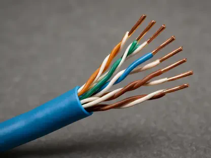
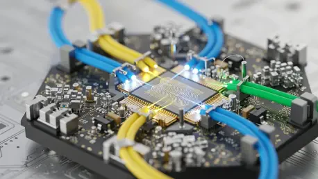
Traditional computing environments have long relied on copper-based electrical interconnects, yet these systems now face a daunting “interconnect bottleneck.” As signals travel through copper at high frequencies, they suffer from significant attenuation and electromagnetic interference, requiring massive amounts of power just to maintain signal integrity. Optical technology bypasses these physical constraints by using light as the primary carrier for data transmission. By integrating photonic components directly into semiconductor packages, engineers can achieve a level of bandwidth density that electrical alternatives simply cannot match.
The relevance of this shift is most visible in the high-performance computing sector. Instead of viewing the processor as an isolated island of logic, optical interconnects treat the entire cluster as a fluid network. This integration is essential for training the next generation of neural networks, where the ability to synchronize thousands of processing units determines the viability of the model. Photonic integration represents more than just a hardware upgrade; it is a fundamental redesign of how information moves across the silicon landscape.
Core Features and Architectural Breakthroughs
Scale-Up Photonic Integration and GPU Clustering
One of the most transformative features of this technology is its ability to facilitate massive scale-up architectures. In a typical setup, individual GPUs are often limited by the speed of the bus connecting them, leading to wasted cycles while processors wait for data. Optical interconnects allow these clusters to function as a single, tightly integrated computing unit. By creating a unified photonic fabric, the system maximizes processing power across the entire array, effectively turning a room full of servers into a giant, cohesive supercomputer.
High-Throughput and Low-Latency Performance
The technical superiority of photons over electrons is most evident in performance metrics. Light travels with minimal heat generation and nearly zero signal degradation over the short distances required within a data center. This allows for significantly higher throughput, enabling the transfer of terabits of data per second with latency that is orders of magnitude lower than copper. For AI workloads, where every millisecond of delay during backpropagation adds up to days of lost training time, this low-latency performance is a critical competitive advantage.
Open Protocols and Ecosystem Interoperability
While some industry giants attempt to lock customers into proprietary hardware ecosystems, a significant trend is emerging toward open standards. Leaders in the space are prioritizing vendor-neutral infrastructure, which allows different types of chips and optical engines to communicate seamlessly. This interoperability is vital for hyperscale operators who need to scale their infrastructure without being tethered to a single manufacturer’s roadmap. By adopting open protocols, the industry ensures that optical networking remains a flexible and scalable foundation for diverse AI hardware.
Market Evolution and Current Industry Trends
The financial landscape surrounding optical interconnects has shifted from academic interest to high-stakes commercialization. Specialists like Lightelligence have recently pursued significant public listings, signaling that the technology is ready for prime-time deployment. These moves reflect a broader surge in the semiconductor sector, where investors are pivoting toward the “plumbing” of AI. Private valuations for firms such as Ayar Labs and Lightmatter have reached multi-billion-dollar levels, highlighting a consensus that connectivity is the next great frontier of silicon value.
Market expansion is particularly aggressive in regions with heavy infrastructure investment, such as the Chinese sector, which is projected to see a 100% compound annual growth rate through 2030. This growth is driven by the urgent necessity to modernize data centers to support local AI initiatives. As the market matures, the focus is shifting from niche experimental setups to standardized, mass-produced optical modules that can be integrated into any standard rack, democratizing access to ultra-high-speed data movement.
Strategic Applications in the AI Era
Real-world deployment of optical interconnects is currently centered on managing the massive traffic demands of hyperscale data centers. Large Language Models require constant communication between memory and logic units, a process that traditionally consumes a disproportionate amount of energy. By deploying optical engines, operators can reduce the overall power envelope of their facilities while simultaneously boosting the efficiency of complex workloads. This allows for more compute-intensive tasks to be performed within the same thermal and power constraints of existing buildings.
Unique use cases are also emerging in edge computing and specialized research environments. For instance, optical interconnects are being used to link distributed sensors in real-time, where the high bandwidth allows for immediate processing of massive data streams. These applications demonstrate that the technology is not just for the largest tech companies, but is becoming a foundational tool for any industry that relies on the rapid movement of large datasets, from autonomous vehicle training to genomic sequencing.
Implementation Challenges and Technical Hurdles
Despite its potential, the path to universal adoption is fraught with manufacturing complexities. Producing photonic chips requires a level of precision that exceeds traditional CMOS fabrication, often leading to lower yields and higher costs. Furthermore, while light generates less heat during transmission, the lasers required to power these systems still present thermal management challenges. Integrating these optical engines directly into a chip package—known as co-packaged optics—requires sophisticated packaging techniques that are still being refined for mass production.
Current development efforts are focused on silicon photonics, which aims to use existing semiconductor manufacturing equipment to produce optical components. This would significantly lower the barrier to entry and reduce the high initial costs of deployment. Additionally, researchers are working on hybrid integration methods that place the light source outside the chip to simplify cooling requirements. These technical iterations are necessary to transform optical interconnects from a luxury high-end solution into a standard commodity.
Future Outlook and Global Technological Impact
The trajectory of this technology points toward a transition from raw chip performance to connectivity-centric computing. In the coming years, the distinction between computing and networking will likely blur, leading to architectures where the interconnect is as much a part of the logic as the processor itself. This convergence of optical computing and data movement will redefine the global race for AI supremacy, as the winner will be determined not just by who has the fastest chip, but by who can move data between those chips most efficiently.
Looking forward, the integration of all-optical switches could eliminate the need for costly optical-to-electrical conversions entirely. This would create a “transparent” network where data remains in the form of light from the moment it is generated until it is processed. Such an advancement would represent the final step in the transition to a truly photonic age, drastically reducing the carbon footprint of global digital infrastructure while enabling levels of intelligence that were previously hampered by the physical limits of metal.
Final Assessment of Optical Interconnects
The shift from traditional electrical signals to light-based data movement has redefined the parameters of what is possible in modern computing. It was clear that the limitations of copper were no longer sustainable for the demands of 2026, and optical interconnects stepped in as the necessary successor. This review found that while manufacturing hurdles remained a significant barrier to entry, the performance gains in latency and bandwidth density provided an undeniable justification for the investment. The technology successfully bridged the gap between theoretical processing power and practical, scalable AI infrastructure.
Ultimately, the move toward open protocols and silicon photonics indicated a maturing industry ready for widespread adoption. These advancements ensured that the interconnect bottleneck was no longer the primary constraint on human ingenuity in the field of artificial intelligence. As global players continued to compete for dominance, the adoption of optical technology became the clear differentiator between stagnant legacy systems and the high-efficiency architectures of the future. The transition to light was not merely an incremental upgrade; it was a fundamental requirement for the next era of global digital growth.